IBM squeezes 30 billion transistors into a fingernail-sized chip
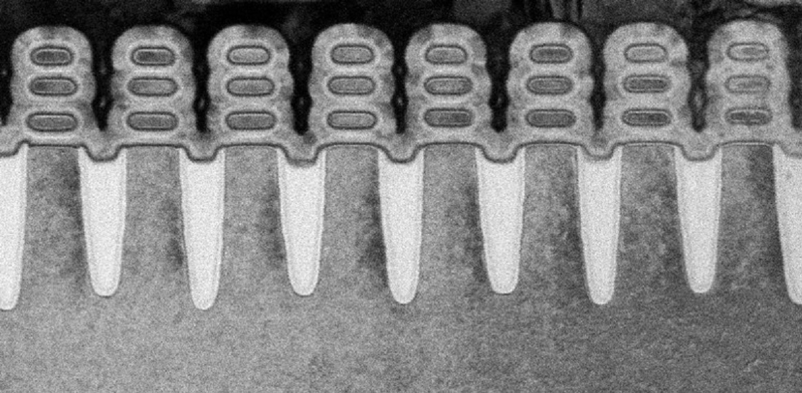
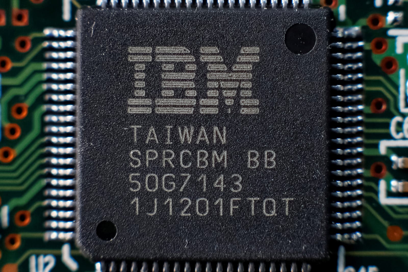
Who said Moore’s Law was dead? Certainly not IBM or its chip partners Globalfoundries and Samsung. The trio has developed a transistor manufacturing process that should pave the way for 5-nanometer chips. While the team etched the chip using the same extreme ultraviolet lithography (EUV) used for the breakthrough 7nm chip, it ditched the common FinFET (fin field effect) transistor design in favor of stacks of silicon nanosheets. The switch makes it possible to fine-tune individual circuits to maximize their performance as they’re crammed into an incredibly small space. How small? At 5nm, the group says it can squeeze 30 billion transistors into a chip the size of a fingernail (see below) — not bad when the 7nm chip held 20 billion transistors a couple of years ago.
IBM sees the technique helping its own cognitive computing efforts as well as the Internet of Things and other “data-intensive” tasks. However, it’s also painting a rosy picture for the future of mobile devices — it imagines phones having “two to three times” more battery life than current devices. That’s likely optimistic (phone makers tend to focus on speed over longevity), but it won’t be shocking if future hardware is both faster and wrings out a little more from every charge.
Just don’t expect to see real-world examples of this for a while. We haven’t even seen devices shipping with 7nm chips (they’re not expected until 2018 at the earliest), so it could easily be a couple of years or more before 5nm arrives. Still, that 5nm is even on the roadmap is important. Chip designers won’t have to reinvent the wheel to get meaningful improvements, and you won’t have to worry about device performance growing stale for at least the next few years.

(34)


